


邓震
简介:
现为中科院物理所副研究员,博士生导师,工作于清洁能源实验室E03组.
2014年7月, 中国科学院物理研究所获得博士学位;
2014年7月-2016年3月, 中国科学院微电子研究所,助理研究员;
2016年3月-2018年5月, 美国耶鲁大学,博士后;
2018年8月, 进入中科院物理所, 副研究员,入选中国科学院物理研究所引进海外杰出人才。
2021年 入选中国科学院青年创新促进会
学术兼职:
2022年-2024年,中国物理学会应用物理前沿推介委员会委员
主要研究方向:
III-V族材料的外延生长及其光电器件研究,III-Nitrides的MOCVD生长及其器件研究,其他新型光电器件的研究。其中外延生长主要涉及到MOCVD及MBE等大型设备;器件制作主要涉及到微纳加工设备及工艺。
过去的主要工作及获得的成果:
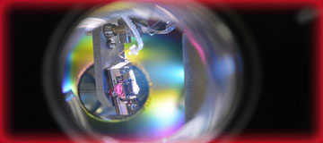
1.针对光的偏振成像,并结合亚波长光栅制备技术,片上集成了一种台面型InGaAs/InP基PIN短波红外偏振探测器原型器件。该原型器件具有的深台面结构可以有效地防止电串扰,使其潜在地实现更小尺寸短波红外偏振探测器的制备[Optics Letters, 47,6173(2022)];研究过短波红外面阵探测器小像元之间的暗电流抑制及串扰问题[Results in Optics, 5, 100181 (2021)];研制出一种基于 III-V化合物半导体材料的可见-短波红外宽光谱柔性光电探测器[Scientific Reports,12,7681(2022) ];设计一种针对中波红外探测的高数值孔径和量子效率的超透镜[Optics Letters, 49, 5563 (2024)]。
2.针对实现全硅基探测器1.1μm以上的红外探测难题,提出了利用纳米厚度Au薄膜与ITO复合结构,实现了低暗电流密度的硅基短波红外光电探测器制备,为光通信中全Si基光电探测单片集成提供重要技术支撑[Photon Res., 8, 1662(2020);Sensors, 22,4536(2022)];
3. 针对更高性能LED的应用需求,提出若干种提高LED光电性能的新方法,为获得高效蓝绿光LED提供了技术支撑[Sci.Rep.3,3389(2013);Sci. Rep., 4,6734(2014);Phys. Status Solidi A, 211,1175(2014)];
4.面向GeSi合金基板在Si基光电子领域的应用需求,提出了一种电化学腐蚀和气相分子束外延技术相结合的方法,实现了Ge组分及基板厚度均可调谐的GeSi合金,为Si基光电单片集成提供了坚实的基础[Jpn. J. Appl. Phys. 59, 050904(2020);Chin. Phys. B, 30,096104(2021)]。
代表性论文及专利:
到岗(物理所)后发表文章摘选
- F. Meng, J. LIU, J. YUE, L. QIN, J. ZHANG, X. LI, C. SONG, Z. ZHANG, H. CHEN, Y. CHANG, AND Z. DENG*, Design of a polarization-insensitive broadband achromatic metalens for mid-wave infrared detector. Optics Letters, accepted,DOI: 10.1364/OL.541487,2024.(通讯)
- J. Zhang, Z. Gao, M. Wang, G. Ding, C. Du, Y. Jiang, H. Jia, W. Wang, H. Chen, Z. Deng*.Opto-electrical and polarization performance of mesa-structured InGaAs PIN detector integrated with subwavelength aluminum gratings. Optics Letters, 47,6173,2022.(通讯作者)
- X. Li, Z. Deng*, et al., Hybrid nano-scale Au with ITO structure for a high-performance near-infrared silicon-based photodetector with ultralow dark current. Photonics Research, 8, 1662, 2020.(通讯作者)
- W. Wang, Z. Deng*, et al., Dark current investigation in individual planar In0.53Ga0.47As/InP detector and fine pixel-pitch array with spacing variations. Results in Optics, 5, 100181,2021.(共同通讯)
- W. Wang; Y. Li; J. Zhang; Z. Deng*, et al., Influence of Sb2 soaking on strained InAs0.8Sb0.2/Al0.2Ga0.8Sb multiple quantum well interfaces. AIP Advances, 11,075004, 2021.(共同通讯)
- J. Zhang; X. Li; C. Du; Y. Jiang; Z. Ma; H. Chen; H. Jia;W. Wang, Z. Deng*, Experimental Demonstration of the Impact of the Parameters of Floating Guard Ring on Planar InP/InGaAs-based Avalanche Photodiodes’ Performance and its Optimization, IEEE Photonics Journal, 14, 2218406, 2022.(通讯)
- Y. Wang, L. Duan, Z. Deng*, et al., Electrically Transduced Gas Sensors Based on Semiconducting Metal Oxide Nanowires. Sensors, 20, 6781, 2020. (Review,通讯)
- S. Wang, Z. Deng*, et al., Fabrication, structural and optical properties of virtual GeSi template by Ge filling the porous Si prepared by EC etching. Japanese Journal of Applied Physics, 59, 050904, 2020.(共同通讯)
- R. Xu, Z. Deng*, et al., Fabrication of large-scale uniform submicron inverted pyramid pit arrays on silicon substrates by laser interference lithography, Vacuum, 165, 1, 2019.(共同通讯)
目前的研究课题及展望:
在研课题:
1. 国家重点研发项目 科技部 核心参与
2. 中国科学院青促会项目 中科院 主持
3. 173重点项目 JKW 课题负责人
4. XX低噪声放大器项目 JKW 项目负责人
5. 国家基金委青年项目 基金委 主持
6. 揭榜挂帅项目 辽宁省 主持
7. 技术开发项目 其他单位 主持
8. 中科院改善科研条件项目 中科院 核心参与
已结课题:
1. 173重点项目 JKW 课题负责人
2. 中科院物理所人才项目 物理所 主持
3. 技术开发项目 其他单位 主持
培养研究生情况:
每年拟招收1-2名硕博连读生。博士研究生的选题主要偏重于半导体方向的应用基础研究及应用研究。同时欢迎有相关研究背景的博士毕业生来组做博士后!!!学生就业前景较好!!!
其他联系方式:
010-82649296
zhen.deng@iphy.ac.cn
电话:
010-82649296
010-82649053
Email: